-
Lift Ceramic single_layer PDMS SiliconOxide LiquidCrystal FailureAnalysis molecular_self_assembly Polyethylene MeltingPoint CP-AFM Phosphide 3-hexylthiophene Wang Tin sulfide Mobile Bismuth TungstenDeposition PinPointMode thermal_conductivity NeodymiumMagnets Alloy Magnets MoirePattern SKPM Materials PtfeFilter PhthalocyaninePraseodymium nanobar Magnetic NUS_NNI_Nanocore CrystalGrowing Resistance Al2O3 MBE
Report image
If you found this image unacceptable, please let us know. We will review your report and take action if we determine this image is really unacceptable.
Taegeuk Mark Lithography on PZT
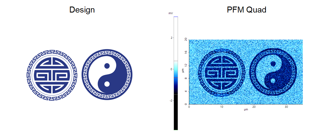
Re-arranged the domain pole direction on PZT surface using bias mode of lithography.
Scanning Conditions
- System: NX10
- Scan Mode: Lithography
- Cantilever: PPP-ContScPt (k=0.2N/m, f=25kHz)
- Scan Size: 35μm×20μm
- Scan Rate: 0.5Hz
- Pixel Size: 1024 × 1024
- Tip Bias: 10V for patterned area
- Scan Mode: Lithography
- Cantilever: PPP-ContScPt (k=0.2N/m, f=25kHz)
- Scan Size: 35μm×20μm
- Scan Rate: 0.5Hz
- Pixel Size: 1024 × 1024
- Tip Bias: 10V for patterned area