-
pulsed_laser_deposition LifeScience Vacuum phase_change MfmPhase ScanningKelvinProbeMicroscopy Pattern BoronNitride Korea LowDensityPolyethylene Polyaniline Aluminium_Oxide Metal-organicComplex LiftHeight Wildtype Jason UnivMaryland Layer DLaTGS blended polymers ForceVolume Melt CrossSection sputter AtomicSteps StyreneBeads Blend temperature controller AFM ScanningTunnelingMicroscopy Pipette Insulator Heating Nanostructure Annealing WWafer
Report image
If you found this image unacceptable, please let us know. We will review your report and take action if we determine this image is really unacceptable.
Trench Etch Profile on Si Wafer
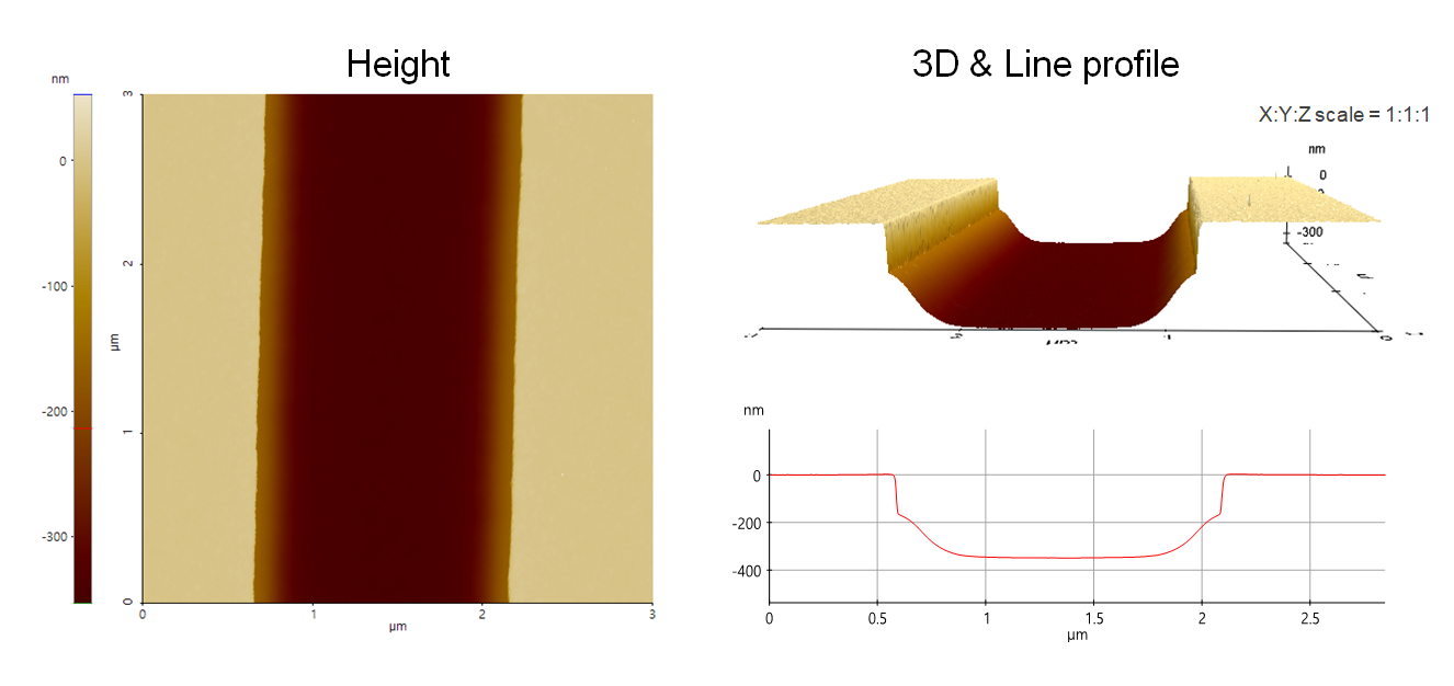
Top dielectric trench etch profile on Si wafer having tapered slope at the trench sidewall.
Scanning Conditions
- System: NX20
- Scan Mode: Non-contact
- Cantilever: AC160TS (k=26N/m, f=300kHz)
- Scan Size: 3μm×3μm
- Scan Rate: 0.21Hz
- Pixel: 1024 × 256
- Scan Mode: Non-contact
- Cantilever: AC160TS (k=26N/m, f=300kHz)
- Scan Size: 3μm×3μm
- Scan Rate: 0.21Hz
- Pixel: 1024 × 256